
DroneNode Motherboards - Evolution from v1 to v5
Each boat (or other device) is based on a custom ESP32-based motherboard running our DroneNode firmware. The motherboard exposes the ESP32 IO interfaces (digital/analog IO, serial, SPI) and includes an 8-channel I2C expander to make connecting peripheral devices extremely easy. It has also evolved to include onboard GPS, RFM69 radio, QMC5883L compass, status Neopixel and micro-SD card reader as of v4.
The same DroneNode firmware runs on all versions of the motherboard, maintaining backward compatibility and auto-detects hardware version based on an I2C scan of onboard devices.
See DroneLink Architecture for how the motherboards fit into the overall DroneLink ecosystem.
Version 1 - Simple beginnings
Our first attempt at a motherboard to support early test boats (like the Paddles) - calling it a motherboard is a stretch, given it was really just a breakout board for an ESP32 DevKit, an I2C multiplexer, and a bunch of connectors for expansion ports / I2C.
Its simplicity was deliberate. It was a good chance for me to get back into PCB design (having barely touched it in over a decade) and serve as a quick/cheap/straightforward platform for further development.
ESP32
Selecting the ESP32 as the long-term platform on the hardware side was an important choice, but a fairly easy one. I've been working with embedded devices for over 20 years and have used most common platforms at some point (ARM, PIC, various Arduinos, etc), but in more recent years, I've settled on ESP32 as my "go-to". It provides an excellent balance of computing power, memory, flash, IO, integrated WiFi/Bluetooth, library/community support, and is extremely low cost. It also had no supply chain issues through COVID, which helped!
I2C
You may be wondering why we included the I2C expander, given I2C can support a lot of devices on a single bus. After early experimentation, it was a choice driven by:
- Some I2C devices have a fixed address and so you can't have multiple on a single bus
- Minimal sensors per bus minimises noise and also generally avoids issues with pull-up resistors
JLCPCB, EasyEDA, and LCSC
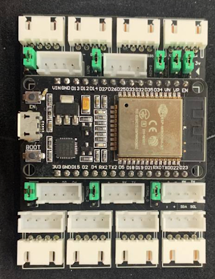
Version 2 - Start of Integration
For Version 2, I wanted to start including surface-mount components (rather than plugging in modules), bring the size down and integrate some common components - starting with the I2C multiplexer and RFM69HW radio module.
Two of our core design principles are modularity and minimal part count, so this motherboard also standardised on 4-pin JST-XH connectors. All external IO was exposed on these 4-pin connectors, each combining a pair of IO pins plus power and ground, with a jumper allowing the power pin to the connected to 5V or 3.3V.
Version 3 - Tried to be too clever, Epic fail
In version 1 and 2 boards, we would occasionally have issues with a sensor that would require a power reset to resolve. Wanting to automate this power reset function, I thought it would be fun to control the power pins for external devices using a bunch of MOSFETS - one for the 3.3V rail and one for 5V rail. Having so many MOSFETS to control needed a lot of IO pins, so I included a 16-port IO multiplexer.
However, once the boards arrived for testing it didn't take long to produce magic smoke. It turned out I'd completely misread the Chinese datasheet for the IO multiplexer and it's bootup state was for all outputs to be active - enabling all the power outputs and shorting the 3.3V and 5V rails. Suffice to say that put a rapid end to the V3 boards and the whole batch went into the reclamation pile. I've since scavenged the occasional chip off them, but basically, they're junk.
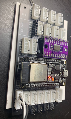
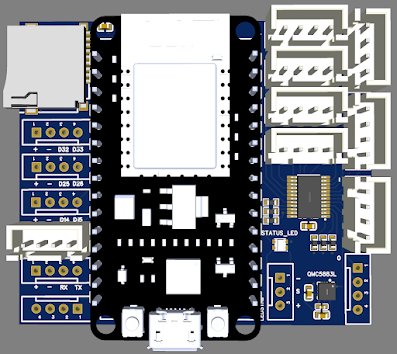
Version 4 - Bells'n'whilstles
On-board I2C multiplexer
On-board RFM69HW with active antenna connection
On-board micro SD card module
On-board GPS with antenna connection - ZHONGKEWEI ATGM336H-5N31 - https://www.icofchina.com/d/file/xiazai/2016-12-05/b5c57074f4b1fcc62ba8c7868548d18a.pdf
On-board compass (i2c) - QMC5883L - https://datasheet.lcsc.com/lcsc/2012221837_QST-QMC5883L_C976032.pdf
Optional voltage divider to analog input for monitoring battery voltage (max 14.2V range to support up to 3S source)
Power selection for expansion/serial ports moved to solder-bridges on back of board to save space
WS2812b status LED leading to header for LED strip (pin D2)
Packed into an even smaller 65mm x 56mm footprint
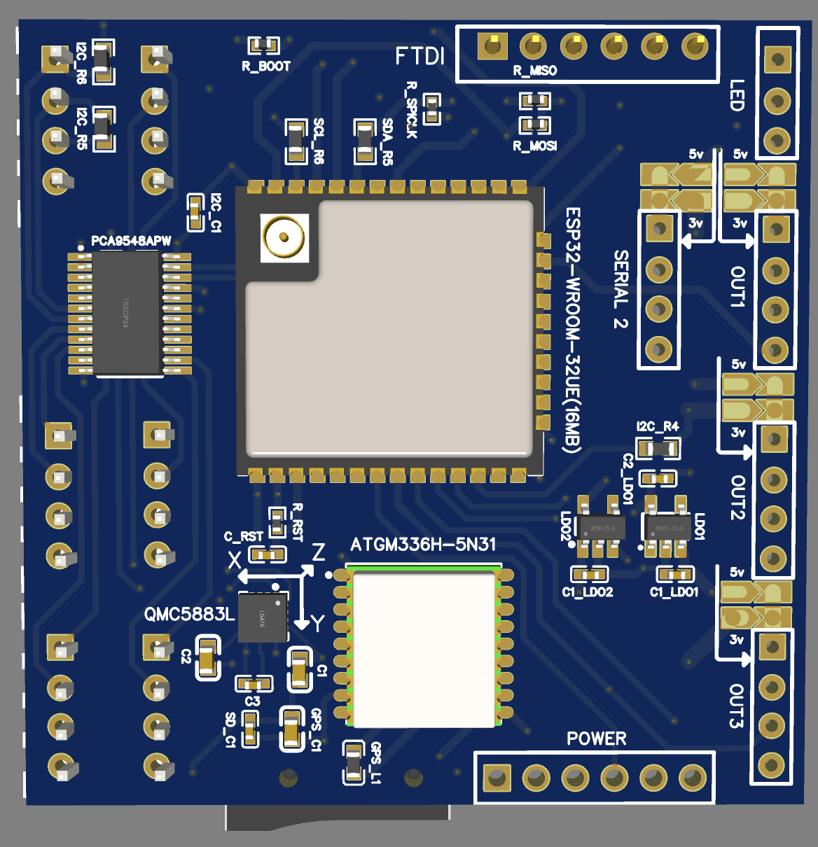
Version 5 - TBC
- Move from using a plug-in ESP DevKit module to onboard ESP SOC and associated circuitry - targeting the ESP32-WROOM-32UE (16MB) Soc with external WiFi antenna for enhanced range
- Header for FTDI programming (no onboard USB interface to save cost/space)
- Shrink board footprint to 50x50mm
- Stackable with the Power Module v2
- Edge JST-XH connectors can be interchanged with right-angled versions for low profile wiring
- Different multiplexer I2C address from v4 to allow for automatic motherboard version detection
- Optional permanently enabled peripheral power or controlled via ESP on D32
- Bottom-side surface mount components to be soldered using a hot plate, including majority of SMT components, especially those with challenging footprints (like the tiny compass)
- Top-side SMT is simple enough to be hand-soldered
- Through-hole connectors are hand-soldered last


Comments
Post a Comment